
Patterned Wafers Explained: Uses, Types, and Fabrication
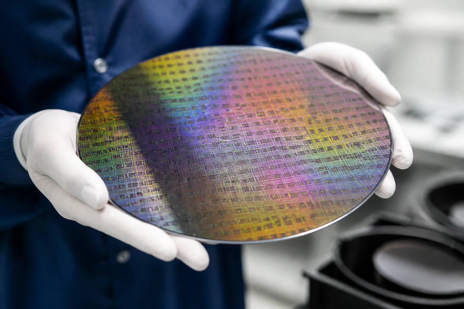
A patterned wafer is a semiconductor wafer with intentionally created surface features such as lines, grids, dots, alignment marks, and device-like geometries. Unlike a bare wafer, it is built for lithography, etching, metrology, overlay verification, inspection, and process development, not just as a starting substrate.
In practice, patterned wafers are used to qualify tools, validate process windows, measure critical dimension, check alignment accuracy, monitor defect detection performance, and study pattern fidelity before full production runs. They appear across semiconductor manufacturing, MEMS, photonics, sensing, and calibration workflows on silicon wafer platforms as well as SiC, GaAs, and sapphire.
What defines a patterned wafer
The defining feature is intentional topography or material contrast created by photolithographic patterning. A patterned wafer contains repeatable structures engineered for a purpose, whether that is a simple line-and-space target for CD-SEM measurement or a full die array with test structure blocks, fiducial patterns, and overlay targets.
These wafers are not limited to advanced logic or memory applications. They are equally important in process monitoring, tool calibration, tool qualification, and R&D programs where engineers need known geometries to compare against measured results.
How they differ from bare wafers
A bare wafer is an unpatterned substrate, often specified by substrate type, orientation, resistivity, diameter, thickness, and polish condition such as single-side polished or double-side polished. It is used as the base material for subsequent device fabrication.
A patterned process wafer adds formed features on that substrate. Those features introduce image complexity for inspection, overlay sensitivity for lithography, and measurable structures for metrology. That distinction matters because patterned and non-patterned inspection are fundamentally different: bare wafer inspection can detect particles directly, while patterned wafer inspection often compares neighboring dies to separate real defects from intended geometry.
Common pattern types
Line and space
Line and space patterns are among the most widely used structures for critical dimension control, etch bias studies, and resist process tuning. They help engineers evaluate linewidth, sidewall transfer, and pattern collapse risk after lithography and etching.
In research settings, patterned silicon wafer samples with line-groove dimensions around 10 to 50 microns are common for instrument setup, fluidic studies, and surface characterization.
Dots and grids
Dot and grid arrays support focus studies, uniformity checks, and defect detection benchmarking. Their regular spacing makes them useful for image-processing validation and for checking whether an inspection system can separate nuisance signals from true defect events.
Alignment features
Alignment marks and fiducial patterns are built for overlay tools and stepper or scanner alignment routines. These structures let engineers measure registration error between layers and verify that exposure tools are placing each patterned layer where it belongs.
Electrical test structures
Many patterned wafers carry dedicated test structure regions instead of full product designs. These can include resistors, capacitors, transistors, and van der Pauw structures used to extract sheet resistance, contact behavior, leakage, and other electrical parameters without needing a complete finished device.
Device-like geometries
Some wafers are intentionally patterned with die array layouts that resemble production parts. This is useful for process development, defect classification, voltage contrast studies, and qualification of a wafer defect inspection system under realistic pattern density conditions.
Fabrication flow
Most patterned wafers follow a straightforward manufacturing sequence, although the exact stack and tolerances depend on the application.
Select the substrate based on material, diameter, orientation, resistivity, thickness, and polish condition.
Apply photoresist and expose the design through a photomask during lithography or microlithography.
Develop the resist to define the intended geometry.
Transfer the pattern by etching or, in some flows, by deposition and lift-off.
Clean the wafer to remove residues and preserve surface quality.
Verify dimensions, overlay, defects, and surface features through metrology and inspection.
On silicon wafers, dopants can include boron, phosphorus, antimony, or arsenic depending on the required electrical behavior. For specialized applications, patterned wafers are also produced on compound semiconductor wafer materials including GaAs, SiC, and sapphire.
Materials and wafer formats
Silicon remains the standard platform because it supports mature lithography, etching, and metrology workflows. It is also available across a broad range of diameters used in electronics, from 25.4 mm up to 300 mm, with 450 mm demonstrated but not in general use.
Standard silicon thickness examples include 275 μm for 2-inch, 525 μm for 4-inch, 675 μm for 150 mm, 725 μm for 200 mm, and 775 μm for 300 mm wafers. Material selection is driven by the device environment and the process being studied, so silicon carbide, GaAs, sapphire, and other substrates are chosen when thermal, optical, or power-device requirements demand them.
Engineers who build automated review flows often adapt concepts from image search techniques because patterned-wafer inspection depends on recognizing repeat geometry while isolating non-repeating anomalies.
Where patterned wafers are used
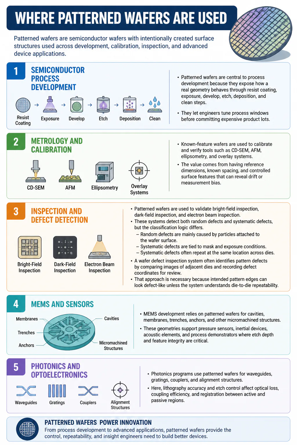
Semiconductor process development
Patterned wafers are central to process development because they expose how a real geometry behaves through resist coating, exposure, develop, etch, deposition, and clean steps. They let engineers tune process windows before committing expensive product lots.
Metrology and calibration
Known-feature wafers are used to calibrate and verify tools such as CD-SEM, AFM, ellipsometry, and overlay systems. The value comes from having reference dimensions, known spacing, and controlled surface features that can reveal drift or measurement bias.
Inspection and defect detection
Patterned wafers are used to validate bright-field inspection, dark-field inspection, and electron beam inspection. These systems detect both random defects and systematic defects, but the classification logic differs.
Random defects are mainly caused by particles attached to the wafer surface.
Systematic defects are tied to mask and exposure conditions.
Systematic defects often repeat at the same location across dies.
A wafer defect inspection system often identifies pattern defects by comparing images of adjacent dies and recording defect coordinates for review. That approach is necessary because intended pattern edges can look defect-like unless the system understands die-to-die repeatability.
MEMS and sensors
MEMS development relies on patterned wafers for cavities, membranes, trenches, anchors, and other micromachined structures. These geometries support pressure sensors, inertial devices, acoustic elements, and process demonstrators where etch depth and feature integrity are critical.
Photonics and optoelectronics
Photonics programs use patterned wafers for waveguides, gratings, couplers, and alignment structures. Here, lithography accuracy and etch control affect optical loss, coupling efficiency, and registration between active and passive regions.
Key specifications to evaluate
Choosing a patterned wafer requires more than asking for a pattern drawing. The wafer has to fit the tool set, the measurement method, and the process objective.
Substrate type: silicon wafer, silicon carbide, GaAs, sapphire, or another platform
Diameter and thickness: matched to handling tools, cassettes, chucks, and process equipment
Orientation: often specified as <100>, <110>, or <111>
Resistivity and doping: relevant for electrical test structure behavior
Polish condition: single-side polished or double-side polished
Pattern class: lines, grids, dots, alignment marks, or device-like geometries
Critical dimension: target width, pitch, depth, and tolerance
Layer purpose: metrology, overlay, inspection, or process monitoring
Patterned wafer types
|
Type |
Typical features |
Primary use |
Main measurements |
|---|---|---|---|
|
CD wafer |
Line and space patterns, dense and isolated lines |
Critical dimension control |
CD-SEM, AFM, profile checks |
|
Overlay wafer |
Alignment marks, box-in-box targets, fiducial patterns |
Alignment and overlay verification |
Overlay tools, registration error |
|
Inspection wafer |
Repeating die array, patterned backgrounds |
Defect detection and classification |
Bright-field, dark-field, electron beam inspection |
|
Electrical test wafer |
Resistors, capacitors, transistors, van der Pauw structures |
Process monitoring and material extraction |
Sheet resistance, leakage, contact behavior |
|
MEMS or photonics wafer |
Trenches, gratings, waveguides, cavities |
Device development |
Depth, profile, optical or mechanical response |
Inspection challenges
Inspection on a patterned wafer is harder than on a dummy bare wafer because the system must separate intentional geometry from true defects. Dense features, repeating edges, and layer-to-layer contrast can all create nuisance events if the recipe is not tuned correctly.
Pattern density also changes how defects appear. A particle on open field may be obvious, while the same particle inside a dense line-and-space block can distort edge contrast, mimic bridge formation, or reduce sensitivity depending on the imaging mode.
Market context
Patterned wafer demand sits inside a large semiconductor wafer market. Worldwide wafer revenue exceeded $11 billion in 2021, and the market is projected to grow more than 6% through 2030, reaching $15 billion.
That growth matters because patterned wafers support lithography, metrology, inspection, and process development before volume manufacturing. They are used to qualify tools, validate overlay performance, monitor critical dimension, and detect both random defects and systematic defects.
Demand is not limited to silicon wafer programs. Patterned substrates are also built on SiC, GaAs, and sapphire for MEMS, sensing, photonic waveguides, gratings, and other device-like geometries that need controlled alignment marks, test structure blocks, and repeatable surface features.
Numeric tolerance examples for common pattern classes
Patterned wafers are specified by measurable geometry, so tolerances are tied to the pattern class, the substrate type, and the intended metrology or inspection use. Common control points include critical dimension, pitch, overlay offset, etch depth, film thickness, and die-to-die placement repeatability.
For research and calibration wafers with line-groove or line and space features around 10–50 microns, engineers usually focus on linewidth consistency, groove depth, and pattern fidelity across the die array. On membrane or device-layer structures, thickness tolerance can be held at ±0.5 μm, with tighter control down to ±0.2 μm in specialized process development flows.
Wafer-level dimensions also follow standard numeric baselines. Standard silicon wafer thicknesses include 275 μm for 2-inch, 525 μm for 4-inch, 675 μm for 150 mm, 725 μm for 200 mm, and 775 μm for 300 mm wafers, while electronics wafers span 25.4 mm to 300 mm in diameter and photovoltaic wafers are commonly 100–200 mm square with thicknesses of 100–500 μm.
Application-specific examples for advanced inspection or metrol
In advanced inspection, a patterned wafer is used to challenge a wafer defect inspection system with realistic surface features instead of a uniform field. Bright-field inspection, dark-field inspection, and electron beam inspection all respond differently to lines, grids, dots, and device-like geometries, so known patterns are essential for tool qualification and defect detection tuning.
Patterned inspection also supports separation of random defects from systematic defects. Random defects are usually particles on the wafer surface, while systematic defects repeat because of photomask, exposure, or process issues and often appear at the same location across a die array.
For metrology, patterned wafers provide known-feature calibration targets for CD-SEM, AFM, ellipsometry, and overlay tools. Engineers use these wafers to verify critical dimension measurement, overlay accuracy, alignment behavior, and pattern fidelity during process development and process monitoring.
FAQ
Is a patterned wafer always made of silicon?
No. Silicon is the most common substrate, but patterned wafers are also fabricated on compound semiconductor wafer materials such as GaAs, SiC, and sapphire when the end use requires different electrical, optical, or thermal properties.
What is the main purpose of a patterned wafer?
The main purpose is controlled evaluation. A patterned wafer gives engineers known structures for lithography, etching, metrology, overlay, alignment, inspection, and process development so they can measure tool and process performance against real geometries.
How is patterned-wafer inspection different from bare-wafer inspection?
Bare-wafer inspection looks directly for particles and surface defects on an unpatterned substrate. Patterned-wafer inspection must account for repeating layout features and often uses die-to-die image comparison to identify non-repeating defects.
What features are commonly included?
Common features include lines, grids, dots, alignment marks, fiducial patterns, test structure regions, and full device-like geometries. The exact choice depends on whether the wafer is intended for metrology, tool qualification, defect detection, or application-specific development.
Are patterned wafers used outside mainstream IC production?
Yes. They are widely used in MEMS, sensors, photonic waveguides, gratings, power-device development on silicon carbide, and specialized research programs that need controlled microfabricated surface features.
What tolerance ranges are typical for different patterned wafer applications?
Tolerance ranges depend on the application, the substrate type, and the metrology method used to verify the pattern. In practice, engineers separate tolerances for wafer geometry, film or etched-feature dimensions, overlay, and test structure electrical behavior rather than treating a patterned wafer as one single-specification part.
For starting material, standard wafer thicknesses are tightly defined by diameter: 275 μm for 2-inch, 525 μm for 4-inch, 675 μm for 150 mm, 725 μm for 200 mm, and 775 μm for 300 mm silicon wafers. Substrate selection also includes orientation, resistivity, and polish condition such as single-side polished or double-side polished.
Feature tolerances vary much more by use case. Research patterned silicon wafer samples with line-groove dimensions around 10–50 microns support less aggressive lithography and metrology work, while CD, overlay, alignment marks, and inspection calibration wafers demand much tighter control of critical dimension, pattern fidelity, and die-to-die repeatability for tool qualification and process development.
What are Solar Wafers?
Solar wafers are semiconductor wafers made for photovoltaic cells rather than integrated circuits. They convert sunlight into electrical energy, so their design priorities differ from a patterned wafer used for lithography, metrology, inspection, or process development in microelectronics.
Unlike round electronics wafers, solar wafers are often produced as square substrates measuring 100–200 mm on a side, with thicknesses of 100–500 μm. Their geometry is optimized for panel packing efficiency and high-area light collection instead of die array layout.
In semiconductor manufacturing terms, a solar wafer is still a substrate, but it is not usually discussed as a patterned process wafer for overlay, alignment marks, or critical dimension control. Its processing emphasizes surface quality, texturing, doping, and cell formation rather than device-like geometries for CD-SEM, AFM, or wafer defect inspection system qualification.
How do specific pattern densities affect inspection recipe tuning in different tool modes?
Pattern density changes both signal behavior and nuisance sensitivity in wafer defect inspection. Dense lines, grids, and dot arrays create stronger background pattern content, so recipe tuning must separate intended geometry from random defects and systematic defects without suppressing real defect detection.
In bright-field inspection, dense periodic features can reduce contrast between the pattern and a small defect. Recipes often need tighter die-to-die or cell-to-cell comparison settings, careful threshold control, and pattern-aware filtering so repeating structures are not misclassified as defects.
In dark-field inspection, dense topography and edge-rich layouts scatter more light, which raises background noise. That pushes recipe tuning toward angle selection, sensitivity balancing, and nuisance rejection tuned to surface features, especially where pattern fidelity, etch roughness, or residue can resemble true defects.
Electron beam inspection is more tolerant of complex device-like geometries, but higher pattern density increases review time and data volume. Recipe setup must account for voltage contrast response, charging behavior, and critical dimension variation across the die array so the tool can isolate localized defects from normal process variation.
Lower-density patterns, such as isolated alignment marks, fiducial patterns, or sparse test structure blocks, are easier to segment but can expose edge-placement and overlay errors more directly. For these wafers, recipe tuning often emphasizes alignment stability, overlay sensitivity, and coordinate accuracy rather than aggressive background suppression.
During process development, engineers commonly tune recipes across multiple pattern classes on the same patterned wafer: dense line and space arrays for CD monitoring, intermediate grids for process monitoring, and open-field regions for particle inspection. That mix helps qualify how each inspection mode responds before production recipes are released.
Conclusion
If the goal is to evaluate a real manufacturing step, a patterned wafer is the right vehicle. Start with the process question first, then define the substrate type, pattern class, critical dimension, and inspection or metrology method so the wafer design directly supports the decision you need to make.