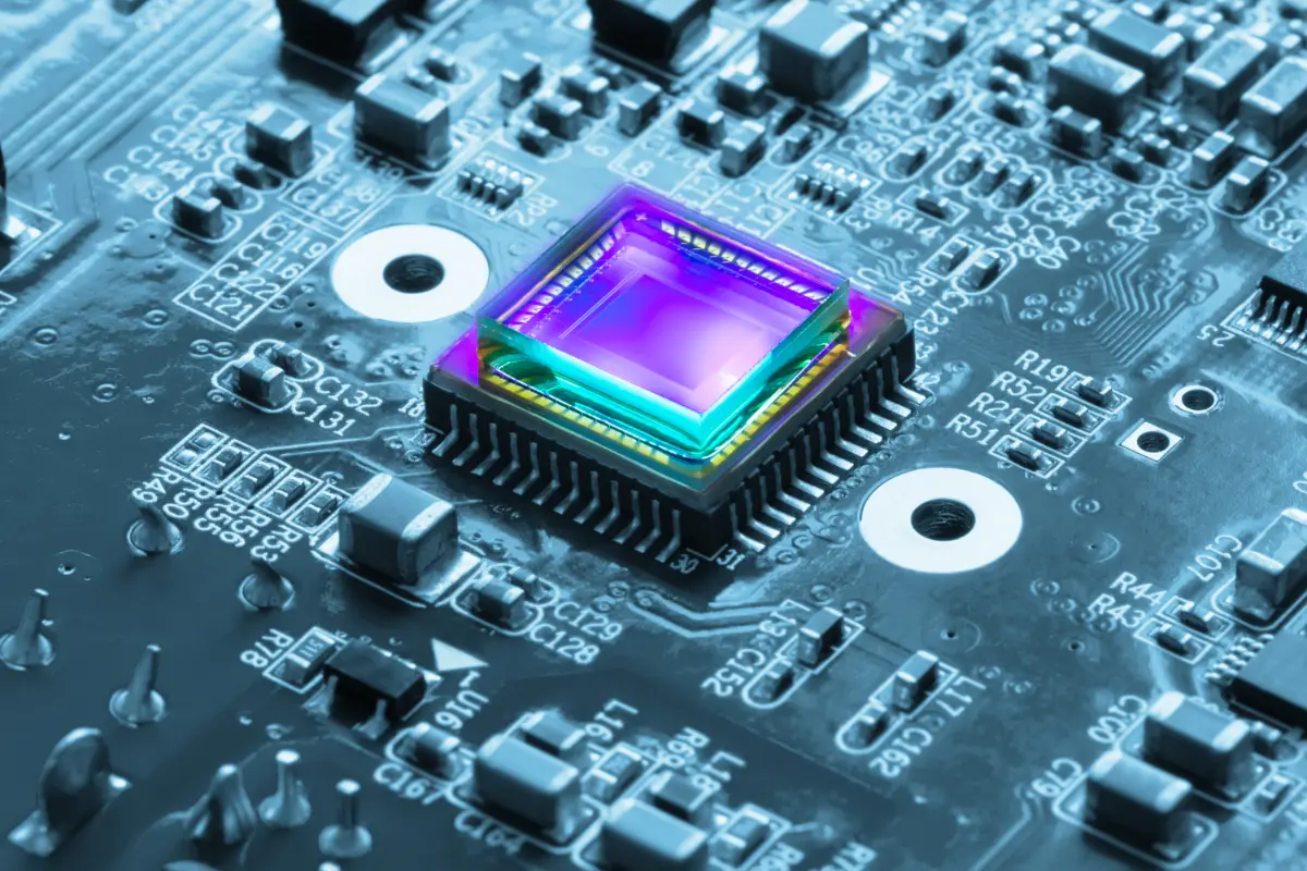
What Are the Design Rules for High-Speed PCB Layouts?
In today’s fast-paced technological landscape, high-speed PCB layouts play a crucial role in the performance of electronic devices. With data rates skyrocketing and component sizes shrinking, adhering to specific design rules becomes essential for ensuring signal integrity and minimising electromagnetic interference. This article delves into the key design principles that engineers must consider when creating high-speed PCBs, highlighting their importance in achieving reliable and efficient electronic systems.
Importance of High-Speed PCB Layouts
High-speed PCB layout plays a crucial role in modern electronics. They ensure signal integrity, power integrity, and electromagnetic compatibility (EMI/EMC) in high-speed digital systems. With the rise of higher data rates and smaller components, the potential for signal degradation and interference increases. Effective design reduces these risks, enhancing overall performance. To achieve optimal results, many engineers rely on electronic design services to fine-tune layouts, minimize signal losses, and ensure compliance with industry standards.
Maintaining signal integrity is essential for reliable communication in electronic devices. Signal integrity involves preserving the quality and timing of signals as they travel through traces on the PCB. Any degradation can lead to data errors, impacting device functionality.
Power integrity ensures that power distribution remains stable and that voltage levels stay within acceptable thresholds across the board. This stability prevents issues like voltage sag and ripple, which can adversely affect the operational capabilities of the circuit.
EMI/EMC considerations are vital for preventing interference between different components and systems. High-speed PCB layouts must incorporate strategies to minimize electromagnetic interference, safeguarding device performance.
Rigorous design rules for high-speed PCBs contribute to their reliability and effectiveness in critical applications. Adhering to these principles shapes the functionality and longevity of electronic devices.
Key Design Rules

High-speed PCB layouts require meticulous attention to specific design rules to improve performance and reliability. Following these guidelines ensures optimal signal integrity, minimises electromagnetic interference, and maintains overall system efficiency.
Impedance Control
Impedance control is vital for high-speed PCB designs. Designers should match impedance values for traces to avoid reflections and signal degradation. Typically, a controlled impedance value of 50 ohms is standard for single-ended signals, while 100 ohms is standard for differential pairs. Utilising proper trace widths and spacing helps maintain consistent impedance throughout the PCB.
Trace Length and Width
Trace length and width significantly impact signal integrity. Designers must limit trace lengths to reduce signal delay and distortion, especially in high-frequency applications. For trace width, maintaining a minimum width of 0.25 mm enhances current-carrying capacity, while also aiding in impedance control. Shorter and wider traces facilitate efficient signal transmission with minimised losses.
Layer Stack-Up
Layer stack-up plays a critical role in PCB performance. Designers should establish a balanced stack-up with alternating signal and ground planes. Utilizing at least four layers can improve signal integrity and reduce crosstalk. Placing power and ground planes close to signal layers helps achieve better electromagnetic compatibility and reduces EMI.
Signal Integrity Considerations
Signal integrity plays a critical role in high-speed PCB layouts. Maintaining signal quality prevents issues that can arise from improper design choices. Key considerations include transmission line effects, frequency impacts, and the length of transmission mediums.
Minimizing Crosstalk
Minimising crosstalk is essential for achieving reliable signal transmission. Designers should route digital signals over a continuous ground plane. This configuration reduces inductive coupling and enhances signal isolation between traces. Additionally, maintaining adequate spacing between signal traces optimises performance by minimising interference. Using differential signalling is another effective strategy, as it cancels out noise and improves data integrity.
Managing Ground Planes
Managing ground planes is vital for minimising electromagnetic interference and ensuring stable reference voltages. Designers should use a solid ground plane to provide a low-impedance return path for signals.
Proper grounding practices reduce ground bounce and improve overall signal integrity. Segregating digital and analog grounds also enhances performance by reducing the risk of cross-domain interference. Careful attention to via placement and minimising ground loop areas further strengthens ground plane effectiveness.
Design Tools and Technologies
Design tools and technologies play a crucial role in the development of high-speed PCB layouts. These resources improve efficiency, accuracy, and performance in the design process.
Simulation Software
Simulation software allows designers to analyse electrical performance before manufacturing. It provides features for modelling signal integrity, power integrity, and crosstalk. Tools like Cadence, Altium Designer, and ANSYS Designer facilitate the evaluation of PCB prototypes, helping identify potential design flaws early. Using simulation software reduces development time and costs while ensuring the final design meets high-speed performance requirements.
Design Automation Tools
Design automation tools streamline the PCB design process. These tools include features for automatic routing, footprint generation, and design rule checks. They help automate repetitive tasks, minimising human error and improving design efficiency.
Popular tools, such as Mentor Graphics and KiCAD, offer extensive libraries and customizable options, allowing designers to adapt their workflows. Implementing design automation tools enhances productivity and ensures adherence to high-speed PCB layout guidelines.
Conclusion
Mastering the design rules for high-speed PCB layouts is essential for achieving optimal performance in today’s fast-paced electronics landscape. By focusing on key aspects like impedance control and effective layer stack-up strategies, designers can significantly improve signal integrity and minimise interference.
Leveraging advanced design tools and simulation software not only streamlines the design process but also ensures that the final product meets rigorous performance standards. As technology continues to evolve, staying informed about the latest design practices will empower engineers to create reliable and efficient high-speed PCBs that meet the demands of modern applications.
FURTHER READING


