
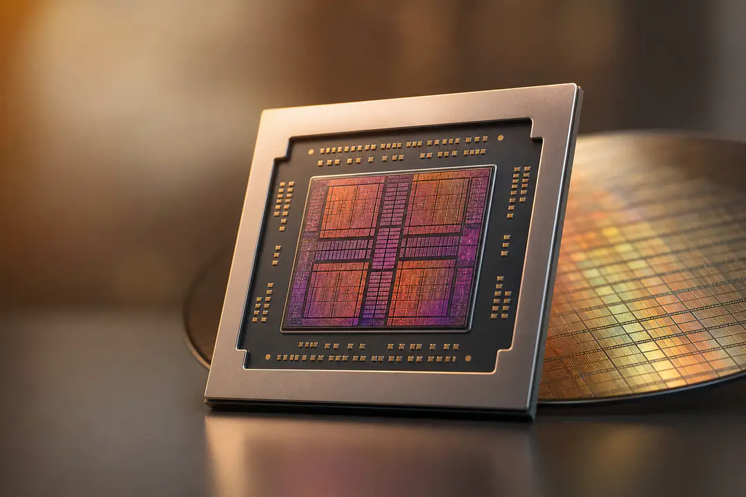
AMD Zen 7 CCD Tipped for TSMC A14 Node
AMD’s Zen 7 roadmap has come into sharper focus after fresh supply-chain chatter pointed to Zen 7 “Grimlock” CCDs on TSMC A14, the foundry’s 1.4nm-class process technology, with launch timing centered on 2028. The reported shift ties AMD’s next major CPU core jump to TSMC’s most advanced node after N2 and N2X, while also suggesting bigger CCDs, more L3 cache, and new packaging choices for desktop CPUs, laptop CPUs, and EPYC parts.
Zen 7 on TSMC A14
The headline claim is straightforward: AMD’s Zen 7 CCD is being prepared on TSMC A14 rather than on a derivative of the N2 family. A14 is the semiconductor maker’s 1.4nm node, scheduled for mass production in 2028, and TSMC has already outlined it as the successor to its 2nm platform for AI, HPC, and mobile designs.
That puts Zen 7 on a more aggressive process technology path than Zen 6. AMD has already placed Zen 6 on TSMC N2, while Zen 7 on a future node was left open on the company’s longer-term CPU roadmap. The latest leak fills in that blank, though AMD has not publicly confirmed node choice, die layout, or product segmentation for Grimlock.
- Zen 7 is linked to the Grimlock codename.
- The CCD is tipped to use TSMC A14, a 1.4nm-class process.
- Timing lines up with TSMC A14 mass production in 2028.
- Zen 6 remains the nearer step, built on N2.
TSMC has also said A14 development is ahead of schedule and has outlined performance and power gains versus N2. Those foundry disclosures do not mention AMD by name, but they establish that the node AMD is rumored to target should exist on the right timeline for a 2028 CPU program.
Cores and Cache
The most striking reported change is a denser CCD. Zen 7 Grimlock is tied to compute dies carrying up to 16 CPU cores each, which would double the familiar 8-core CCD structure AMD has used across several Ryzen and EPYC generations.
Cache is the second major point. The reported ceiling is 224MB of L3 cache per CCD when paired with a 3D V-Cache tile. If accurate, that signals another large step in cache stacking strategy, especially for high-end desktop and server parts that benefit from larger local data pools.
Reported Zen 7 CCD specs
- Up to 16 CPU cores per CCD
- Up to 224MB of L3 cache with a 3D V-Cache tile
- Grimlock desktop parts scaling to two CCDs
- A larger I/O die paired with the compute chiplets
For desktop CPUs, that design opens the door to a 32-core consumer part using two 16-core CCDs. On the server side, the same CCD strategy would give EPYC successors far more flexibility in scaling core counts without proportionally increasing package complexity. It would also fit AMD’s practice of reusing core chiplets across client and data center lines.
AMD has only publicly said Zen 7 will bring a new MATRIX engine and more AI Data formats support. The leak adds the missing physical building blocks: bigger CCDs, more L3 cache, and a stronger tie between CPU cores and advanced packaging.
A14 and Packaging
Node choice is only part of the story. The same reports connect Zen 7 to FOPLP, short for fan-out panel-level packaging, alongside ongoing use of 3D V-Cache and other advanced packaging techniques. That combination points to AMD looking for lower package cost, better routing density, or both, especially as chiplet counts and I/O demands keep rising.
FOPLP has become more relevant as AI and HPC designs push package size, thermals, and interconnect limits. For CPUs, the practical value is not only space savings. It can also shape how AMD places CCDs, cache die, and I/O logic while feeding everything through Infinity Fabric at higher bandwidth targets.
- 3D V-Cache remains central to cache scaling.
- FOPLP would add a new packaging option for chiplet layouts.
- Backside power delivery is part of the broader foundry race, though not confirmed for Zen 7.
- Advanced packaging choices increasingly affect cost, yields, and power delivery.
TSMC has already previewed future platform enhancements with backside power delivery for AI and HPC applications beyond A14. Intel is pursuing a parallel strategy with Intel 18A and the later Intel 14A roadmap, so AMD’s foundry and packaging choices will be watched closely for signs of how it plans to balance performance, thermals, and supply security.
Packaging methods and production flow matter here much like they do in broader manufacturing efficiency trends, because Zen 7’s node story also depends on how AMD packages and routes increasingly complex chiplet designs.
Roadmap context
Zen 7 sits one generation after Zen 6, which AMD has already framed as its N2-era design for Ryzen and EPYC. The leak fits that sequence cleanly in AMD’s public roadmap: Zen 6 arrives first, then Zen 7 takes the bigger architectural step, and Zen 8 follows later.
| Generation | Status | Process tie-in | Key roadmap note |
|---|---|---|---|
| Zen 6 | Officially on roadmap | N2 | Next major client and server generation |
| Zen 7 | Officially named, details undisclosed | TSMC A14 in current leak | New MATRIX engine, future-node design |
| Zen 8 | Future roadmap territory | Undisclosed | Follows Zen 7 in AMD’s long-range plan |
Server timing is also important. Zen 7 EPYC products are widely expected to be early movers for the architecture, with Florence and later server-family naming often discussed in roadmap circles alongside data center deployment plans. AMD tends to prioritize EPYC when a new process or packaging approach promises the largest margin and performance gains.
That lines up with the company’s current push into AI-heavy server designs. Its present-generation roadmap already links EPYC and Infinity Fabric upgrades to accelerator-rich systems, and Zen 7’s MATRIX engine suggests that CPU-side AI acceleration will keep expanding. Similar pressure is visible in AI in smart devices, where chip vendors are also adding more on-die inference features.
Why this matters
If the leak holds up, AMD would be aligning Zen 7 with one of the industry’s most advanced foundry offerings at a time when Intel wants its own 18A and 14A nodes to reset the competitive narrative. For AMD, access to TSMC A14 gives it a path to higher transistor density, lower power, and potentially larger or faster CPU cores without abandoning its chiplet model.
The reported move to 16-core CCDs carries direct product implications. Desktop CPUs could climb to higher core counts with fewer chiplets, while EPYC designs would gain a cleaner path to denser server packages for cloud and enterprise workloads. In data center deployments, more L3 cache per CCD also helps workloads that are sensitive to memory locality, including analytics, database serving, and some AI preprocessing tasks.
- Desktop Ryzen parts could reach higher core counts with less package complexity.
- EPYC could scale core density while preserving chiplet flexibility.
- Larger L3 cache improves performance in cache-sensitive server tasks.
- AMD’s foundry dependence on TSMC would deepen unless a split strategy emerges.
There is also a supply-chain angle. AMD has been linked at times to a broader foundry evaluation that includes Samsung for some future products, but the current Zen 7 CCD talk points squarely to TSMC for the compute chiplets. Even if I/O dies, support silicon, or packaging partners diversify, the leading-edge CPU cores appear tied to TSMC’s roadmap.
Intel, meanwhile, is trying to make Intel 18A relevant sooner and Intel 14A relevant later, with backside power delivery central to its pitch. The gap between process announcements and successful high-volume client or server execution remains the key question for both companies. CPU design choices are also increasingly shaped by inference and orchestration demands tied to AI software platforms, not only by traditional PC benchmarks.
What comes next
The next milestones to watch are trial production progress at TSMC A14, any package-level leaks that clarify FOPLP use, and AMD disclosures around Zen 7’s MATRIX engine, AI Data formats, and Infinity Fabric changes. The broad timeline is already visible: Zen 6 arrives first on N2, TSMC A14 enters mass production in 2028, and Zen 7 follows in that window if the current planning holds.
Until AMD discloses more, the safest reading is that Grimlock marks a serious architectural and manufacturing step rather than a routine shrink. If the rumored 16-core CCD and 224MB L3 cache target are real, Zen 7 will be one of AMD’s most consequential CPU transitions since chiplets became its default design strategy.
The Bottom Line
AMD’s Zen 7 CCD leak points to a bigger change than a simple node update. TSMC A14, larger CCDs, more L3 cache, 3D V-Cache, and FOPLP together suggest AMD is preparing its 2028 CPUs for a market where process technology, packaging, and AI-centric compute blocks all matter at once.